PHOTODETECTOR DEVICES
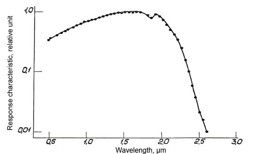
Spectral sensitivity characteristic of the "Photon" photodetector
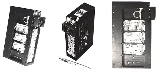
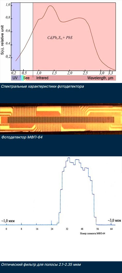
The material is a thin film of the semiconductor Cd1Pb15S16. The sensitive area measures 0.48 × 0.48 mm. It was developed in 1978 for the "Fragment-2" space instrument, operating in the 2.1–2.35 µm spectral range.
Observing Earth from space in the 2.1–2.35 µm spectral range makes it possible to distinguish clouds from snow on the Earth's surface. The "Fragment-2" instrument was launched into orbit in 1980 and operated successfully as part of the Soviet "Meteor-Priroda" No. 3 spacecraft.
Observing Earth from space in the 2.1–2.35 µm spectral range makes it possible to distinguish clouds from snow on the Earth's surface. The "Fragment-2" instrument was launched into orbit in 1980 and operated successfully as part of the Soviet "Meteor-Priroda" No. 3 spacecraft.
NEW SEMICONDUCTORS
We were the First in the World to develop technological processes for the production of ultrapure semiconductors CdPbS (1975) and PbS-st (1985) in the form of a thin film. This allows us to create new versions of photodetectors that are characterized by improved performance and stability.
Our semiconductors turn into a dielectric when cooled, as prescribed for an ideal semiconductor.
Mukhamedyarov, R.D., Beketova, A.A., Stuk, V.I., Mukhamedyarova, G.R. Ultrapure thin films of CdPbS and PbS and photodetectors based on them were obtained and studied for the first time. Indian J Phys 98, 1229–1246 (2024)
ORCID: 0000-0002-8495-6688
Table. Parameters of super structured semiconductor connections in CdS-PbS system.
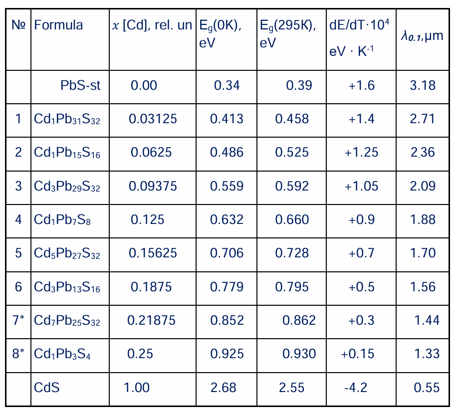
*The possibility of obtaining super structured compounds Numbers 7 and 8 have not yet been experimentally confirmed.
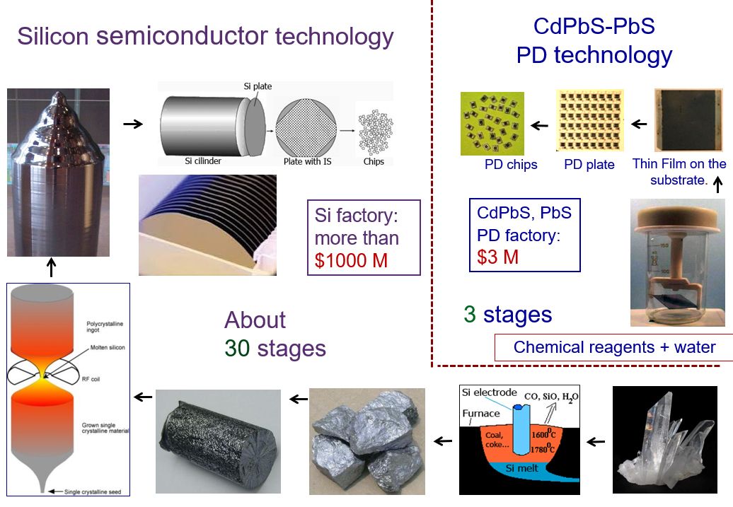
Technology comparsion
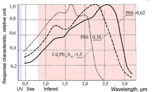
Spectral sensitivity of photodetectors at 295K
The photodetectors are used in flame detectors, pyrometers for temperature measurement, gas analyzers, infrared spectrophotometry.
Data for thin films of different thicknesses, in microns.
PbS-st THIN-FILM PHOTODETECTOR WITH AN IR FILTER AND THE “KONUS” OPEN-FLAME FIRE DETECTOR BASED ON IT
Developed in 1989.
The detector model won first place in a USSR-wide competition in 1990. This prototype served as the foundation for establishing large-scale detector manufacturing in Yekaterinburg under the Pulsar and Spectron brands.
The detector model won first place in a USSR-wide competition in 1990. This prototype served as the foundation for establishing large-scale detector manufacturing in Yekaterinburg under the Pulsar and Spectron brands.
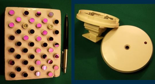
Sigma-5 five-channel photodetector unit
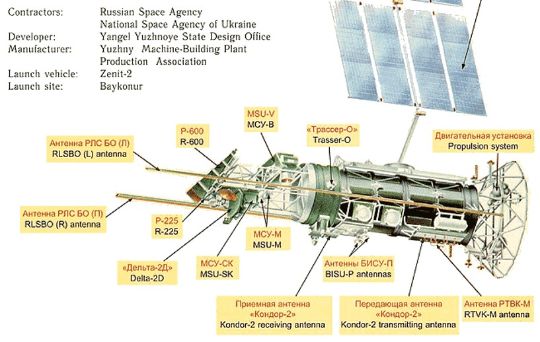
Developed in 1984 for Channel 7 (2.1–2.35 µm) of the MSU-V instrument on the *Ocean-O* spacecraft. The spacecraft has been operating successfully in orbit since July 17, 1999.
https://doi.org/10.1364/JOT.69.000246
"Okean-O" Spacecraft
The main purpose of the spacecraft of this system is to monitor the surface of the World Ocean (the state of the water surface and ice cover).
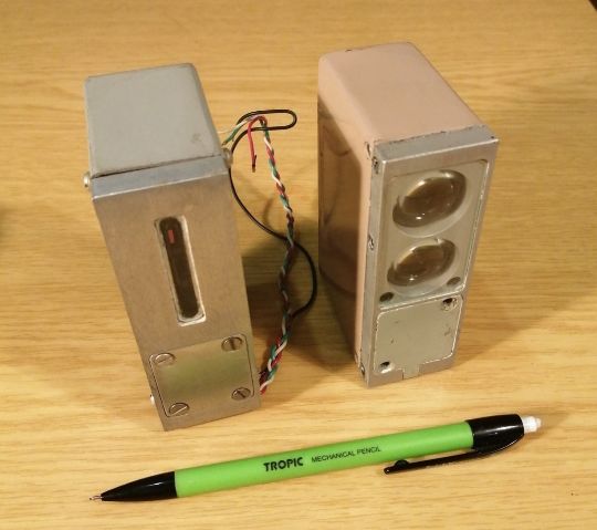
SENSORS BASED ON A SINGLE-ELEMENT PHOTODETECTOR PbS-st
The standard type of photodetector has a time constant of 50–70 µs. This response speed enables the monitoring of processes within a frequency range of 1 Hz to 8 kHz. The second type has a time constant of 8–10 µs, allowing for process monitoring in a range up to 22 kHz.
The first sensor (on the left) is designed to monitor sparking between the brushes and the commutator in high-power electric machines. This allows for the timely detection of wear and the performance of necessary repairs.
The second sensor is designed for the automation of mechanical devices. Its infrared (IR) beam detects the approach of an object or the interruption of the beam when used with a retroreflector.
Using a PbS-st photodetector—as opposed to a silicon (Si) photodiode—significantly improves the performance of the IR beam sensor in conditions of intense ambient light and solar glare. These sensors have also been successfully used during a series of ski competitions in Yekaterinburg (characterized by white snow and dazzling sunlight on the course).
The first sensor (on the left) is designed to monitor sparking between the brushes and the commutator in high-power electric machines. This allows for the timely detection of wear and the performance of necessary repairs.
The second sensor is designed for the automation of mechanical devices. Its infrared (IR) beam detects the approach of an object or the interruption of the beam when used with a retroreflector.
Using a PbS-st photodetector—as opposed to a silicon (Si) photodiode—significantly improves the performance of the IR beam sensor in conditions of intense ambient light and solar glare. These sensors have also been successfully used during a series of ski competitions in Yekaterinburg (characterized by white snow and dazzling sunlight on the course).
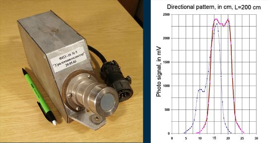
Overheating detector for railway wagon wheelset axle boxes
A thermoelectrically cooled PbSnSe photoresistor is used. The sensitivity range is 3.5–5.0 µm, and the time constant is τ = 12 µs. Replacing the bolometer (τ = 2 ms) allows the device's operating speed to be increased more than 100-fold. The sensor's directional pattern has also been significantly improved. It was developed in 1993. Five units were manufactured for research purposes.
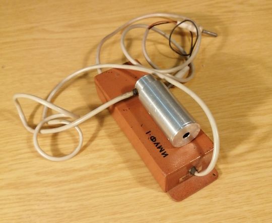
Medical UV laser power meter
A PbS-st photoresistor with a time constant of 8–12 µs is used. The device was designed and manufactured in 1995.
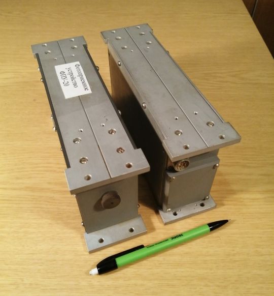
FPU-22 PHOTORECEIVER UNIT BASED ON A PHOTODETECTOR PbS-st-63
It is designed to monitor the molten glass level in a stainless steel canister during the vitrification of radioactive waste. Radiation is transmitted to the device via optical fibers.
Eight FPU-22 sensors monitor the glass-pouring process by simultaneously tracking temperature changes at eight points along the height of the canister wall. This automated system serves as a backup to the primary television monitoring system. Developed in 2007.
The required operational reliability over a period of 15–20 years
is ensured through the use of PbS-st-63 photoresistors
with stable operating parameters.
Eight FPU-22 sensors monitor the glass-pouring process by simultaneously tracking temperature changes at eight points along the height of the canister wall. This automated system serves as a backup to the primary television monitoring system. Developed in 2007.
The required operational reliability over a period of 15–20 years
is ensured through the use of PbS-st-63 photoresistors
with stable operating parameters.
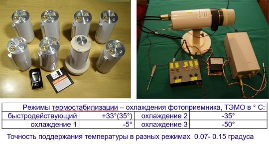
"Sigma-09/U" Universal Photodetector Unit
Measurement of optical radiation power and pulse shape monitoring in the UV, visible, and infrared spectral ranges (0.22–5.0 µm). This is a high-precision, versatile measuring instrument designed for various scientific and industrial applications. Developed in 2009.
PULSED LASER AND LED RADIATION METER (0.22–3.2 ΜM RANGE) BASED ON A PbS-st PHOTODETECTOR
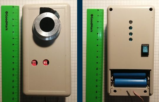
Detection and power measurement of pulses with durations ranging from 1 ns to 5 ms. Powered by two rechargeable batteries; 80-hour operating time.
Used in the laboratory since 2018 for measuring radiation patterns and for the protection of personnel working with ultraviolet and infrared radiation sources.
Used in the laboratory since 2018 for measuring radiation patterns and for the protection of personnel working with ultraviolet and infrared radiation sources.
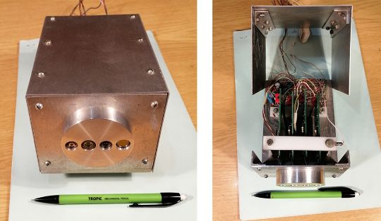
"Triglaz" 4-channel focal plane unit, developed by a student
Designed for the preliminary analysis of the spectral composition of radiation from various sources across the 0.22–3.2 µm range. It incorporates photodiodes covering the UV (220–350 nm), visible (400–750 nm), and near-IR (800–1100 nm) ranges, as well as a PbS photoresistor with an IR filter (1100–3200 nm). Developed in 2022, it is a valuable tool for student education, allowing students to assemble and calibrate the device themselves before conducting measurements.
"Raduga-64" Spectrum Analyzer for Student Training
It is based on our 64-element photodetector, covering the 0.22–3.2 µm range.
Spectral analysis is a fundamental tool in science and industry. It utilizes the entire optical range—from ultraviolet (0.22 µm) to deep infrared (25 µm)—and employs a wide variety of photodetectors based on diverse semiconductor materials.
A 1995 project.
Spectral analysis is a fundamental tool in science and industry. It utilizes the entire optical range—from ultraviolet (0.22 µm) to deep infrared (25 µm)—and employs a wide variety of photodetectors based on diverse semiconductor materials.
A 1995 project.

Photos of the "Raduga-64" analyzer
The "Raduga-64" 64-channel spectrum analyzer (general view). It is akin to a Lego set for teaching optics and electronics: students assemble the device themselves from components on an optical bench and calibrate its operation, subsequently using it to conduct laboratory experiments in physics, chemistry, and biology.
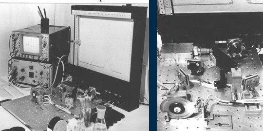
"Raduga-64" spectrum analyzer for student training
An experimental prototype based on a two-layer CdPbS+PbS thin film. It covers a broad optical range of 0.2–3.3 µm, spanning ultraviolet, visible, and infrared (IR) radiation. A photodetector with a 96/128-element array is perfectly adequate for student training; thousands of these need to be produced—enough for every secondary school.
Measurement of emission spectra (Sun, incandescent lamps, flames, glowing coals, LEDs) and transmission spectra (solutions, films, etc.).
Image descriptions (top to bottom):
1. Spectral characteristics of the photodetector;
2. MFP-64 photodetector;
3. Optical filter for the 2.1–2.35 µm band.
1. Spectral characteristics of the photodetector;
2. MFP-64 photodetector;
3. Optical filter for the 2.1–2.35 µm band.
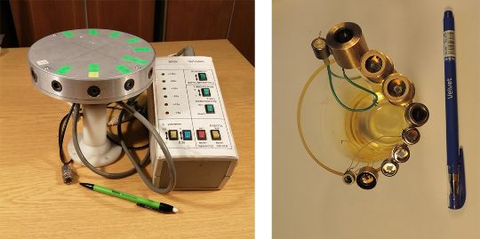
"Quantum Raduga" 10-channel photodetector unit
Designed for measuring radiation across an extremely wide optical spectral range—from 220 nanometers to 15 microns—and for monitoring pulse shapes in the ultraviolet, visible, and infrared ranges; the device utilizes high-speed silicon photodiodes, proprietary CdPbS, PbS, and PbSe photoresistors, and a bolometer.
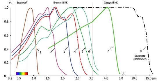
Selection of photodetectors for the "Quantum Raduga" module
Spectral characteristics of photodetectors, in relative units
1–Si PD, 2–Cd1Pb7S8, 3–Cd1Pb15S16, 4–Cd1Pb29S32, 5, 6–PbS, 7–PbSe
1–Si PD, 2–Cd1Pb7S8, 3–Cd1Pb15S16, 4–Cd1Pb29S32, 5, 6–PbS, 7–PbSe
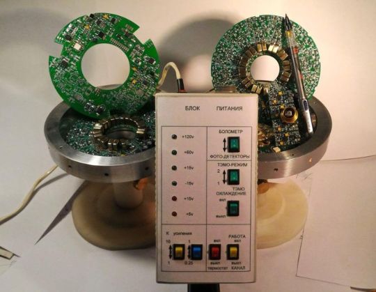
"Quantum RaDUGA" device with control and power supply unit
A versatile tool for photonics tasks—ranging from the development of new devices and measurements in research and manufacturing to the fostering of creative skills.
Capabilities for rapid physical prototyping.
The photodetectors and "Quantum Raduga" modules have individually undergone industrial validation in various devices.
"Quantum Raduga" construction kits offer an intuitive way to explore optics and electronics. They enable the visualization of optical radiation and facilitate research and laboratory work across a wide range of disciplines.
Capabilities for rapid physical prototyping.
The photodetectors and "Quantum Raduga" modules have individually undergone industrial validation in various devices.
"Quantum Raduga" construction kits offer an intuitive way to explore optics and electronics. They enable the visualization of optical radiation and facilitate research and laboratory work across a wide range of disciplines.
Panoramic flame source direction finder for open terrain
Features a number of innovative design solutions. Low power consumption; solar-powered operation.
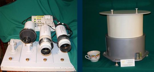
The scanning direction finder is designed to detect the source of a fire and identify signs of equipment failure based on sudden temperature changes. It utilizes four spectral channels within the 1–5 µm range. It can be installed on fire lookout towers or on ships for navigation in fog. It can also serve as the vision system for a mobile security robot. Shown on the right are single-channel devices used to characterize the radiation emitted by actual objects.
The scanning direction finder is designed to detect the source of a fire and identify signs of equipment failure based on sudden temperature changes. It utilizes four spectral channels within the 1–5 µm range. It can be installed on fire lookout towers or on ships for navigation in fog. It can also serve as the vision system for a mobile security robot. Shown on the right are single-channel devices used to characterize the radiation emitted by actual objects.
Nanofilms of ultra-pure semiconductor material. New manufacturing process. Tooling. Testing and measurement equipment.
Protected by 37 official patents.
There are also over 20 cutting-edge developments.
 — Бесплатные Сайты и CRM.